Photonics Automated Assembly & Testing

SKU:
Assemblyline - Automated die-level photonic device assembly https://www.ficontec.com/machine-platforms/#assemblyline Customline - Flexible, Multi-purpose álign-&-attach'platform https://www.ficontec.com/machine-platforms/#customline Testline - Fully automated die-level photonic device test https://www.ficontec.com/machine-platforms/#testline Wafer Testline - Fully automated electro-optical wafer-level device test https://www.ficontec.com/machine-platforms/#wafer-testline Stackline - Laser Bar stacking https://www.ficontec.com/machine-platforms/#stackline Laser Weld - An automated microwelding station for photonics https://www.ficontec.com/machine-platforms/#laser-weld

Assemblyline – Automated die-level photonic device assembly
https://www.ficontec.com/machine-platforms/#assemblyline

Customline – Flexible, Multi-purpose álign-&-attach’platform
https://www.ficontec.com/machine-platforms/#customline

Testline – Fully automated die-level photonic device test
https://www.ficontec.com/machine-platforms/#testline

Wafer Testline – Fully automated electro-optical wafer-level device test
https://www.ficontec.com/machine-platforms/#wafer-testline

Stackline – Laser Bar stacking
https://www.ficontec.com/machine-platforms/#stackline

Laser Weld – An automated microwelding station for photonics
https://www.ficontec.com/machine-platforms/#laser-weld

Assemblyline - Automated die-level photonic device assembly

Assemblyline - Automated die-level photonic device assembly

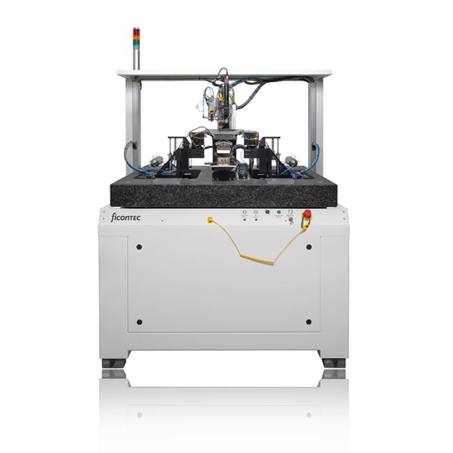
ASSEMBLYLINE systems are fully automated ‘align-&-attach’ assembly systems for the production of optoelectronics and photonic devices. They uniquely combine high-precision optical alignment capability with epoxy-based attachment, eutectic die bonding and/or laser soldering for all optical elements, waveguides, fiber types and die, chip or PIC hybridization tasks – all in an industry-proven design.

Customline - Flexible, Multi-purpose álign-&-attach'platform

Customline - Flexible, Multi-purpose álign-&-attach'platform

CUSTOMLINE is a highly capable development and/or batch processing platform for customers in the semiconductor and photonics packaging market. More than any other ficonTEC product, these systems combine high-precision optical alignment capability with a multiplicity of assembly technologies – including epoxy-based attachment, eutectic die bonding and laser soldering.

Testline - Fully automated die-level photonic device test

Testline - Fully automated die-level photonic device test

TESTLINE production systems are fully automated solutions for electro-optical testing of optoelectronic devices and of singulated PICs (passive/active). Other complex tasks include LIV, spectral and near/far-field beam characterization of single laser chips (incl. VCSELs), unmounted laser diode bars and chip-on-submount (CoS) sources. Lastly, TESTLINE systems can be routinely equipped to also perform detailed optical facet inspection using Deep Learning for defect recognition.

Wafer Testline - Fully automated electro-optical wafer-level device test

Wafer Testline - Fully automated electro-optical wafer-level device test

The WAFER TESTLINE product line is specially designed as a versatile electro-optical test-&-measurement system platform for wafer-level photonic device test. A re-configurable probe-wafer layout even caters to multiple PIC designs on a multi-project wafer (MPW).

Stackline - Laser Bar stacking

Stackline - Laser Bar stacking

STACKLINE systems have been uniquely designed to provide fully automated device stacking and/or unstacking capabilities. This is realized by drawing together selected capabilities from the ficonTEC packaging toolbox – our ubiquitous machine vision system referencing and component recognition/handling, ASSEMBLYLINE’s passive alignment routines, and Testline’s AI-based defect recognition facet inspection procedures. Seamlessly managed by a common process-oriented control interface, the result is an industry qualified and flexibly programmable stacking/unstacking system that continues to see wide usage.

Laser Weld - An automated microwelding station for photonics

Laser Weld - An automated microwelding station for photonics

LASER WELD systems are fully automated ‘align-&-attach’ microwelding production cells for photonics. These systems are typically used for optical assembly and for coupling light out of photonic device packaging (butterfly, TO, custom), using for example, either ferruled optical components or single/multi-fiber coaxial assemblies.

Brands

Loading...

Assemblyline - Automated die-level photonic device assembly

ASSEMBLYLINE systems are fully automated ‘align-&-attach’ assembly systems for the production of optoelectronics and photonic devices. They uniquely combine high-precision optical alignment capability with epoxy-based attachment, eutectic die bonding and/or laser soldering for all optical elements, waveguides, fiber types and die, chip or PIC hybridization tasks – all in an industry-proven design.

Customline - Flexible, Multi-purpose álign-&-attach'platform

CUSTOMLINE is a highly capable development and/or batch processing platform for customers in the semiconductor and photonics packaging market. More than any other ficonTEC product, these systems combine high-precision optical alignment capability with a multiplicity of assembly technologies – including epoxy-based attachment, eutectic die bonding and laser soldering.

Testline - Fully automated die-level photonic device test

TESTLINE production systems are fully automated solutions for electro-optical testing of optoelectronic devices and of singulated PICs (passive/active). Other complex tasks include LIV, spectral and near/far-field beam characterization of single laser chips (incl. VCSELs), unmounted laser diode bars and chip-on-submount (CoS) sources. Lastly, TESTLINE systems can be routinely equipped to also perform detailed optical facet inspection using Deep Learning for defect recognition.

Wafer Testline - Fully automated electro-optical wafer-level device test

The WAFER TESTLINE product line is specially designed as a versatile electro-optical test-&-measurement system platform for wafer-level photonic device test. A re-configurable probe-wafer layout even caters to multiple PIC designs on a multi-project wafer (MPW).

Stackline - Laser Bar stacking

STACKLINE systems have been uniquely designed to provide fully automated device stacking and/or unstacking capabilities. This is realized by drawing together selected capabilities from the ficonTEC packaging toolbox – our ubiquitous machine vision system referencing and component recognition/handling, ASSEMBLYLINE’s passive alignment routines, and Testline’s AI-based defect recognition facet inspection procedures. Seamlessly managed by a common process-oriented control interface, the result is an industry qualified and flexibly programmable stacking/unstacking system that continues to see wide usage.

Laser Weld - An automated microwelding station for photonics

LASER WELD systems are fully automated ‘align-&-attach’ microwelding production cells for photonics. These systems are typically used for optical assembly and for coupling light out of photonic device packaging (butterfly, TO, custom), using for example, either ferruled optical components or single/multi-fiber coaxial assemblies.
Related Product

No data was found